
11 KiB
Multi-Functional Controller (MFC)






A custom, modular remote controller and telemetry station engineered from scratch for long-range, low-latency 2.4 GHz RC control and USB/Bluetooth HID gaming.
Built around the ESP32-S3-N16R8 (Xtensa® 32-bit LX7 dual-core @ 240 MHz), this project is developed in structured hardware phases—starting from a hand-wired 6×9 cm perfboard carrier core and scaling into a full desktop/console transmitter housed in a DT-100 (190 × 137 × 59 mm) instrument enclosure.
Phase 1: Core Carrier Board Showcase (Current Build)
The current physical hardware implements the Core MCU & RF Carrier Stage on a 6×9 cm perfboard:
- ESP32-S3-N16R8 Microcontroller (socketed on female headers)
- nRF24L01+ 2.4 GHz RF Transceiver Module with external dipole SMA antenna
- 100 µF Electrolytic Decoupling Capacitor (
C1) across the 3.3V/GND radio rails to suppress TX burst voltage droop - Modular Male Pin Headers & Dedicated Power Rail Headers for external display, encoder, and joystick breakout interfacing
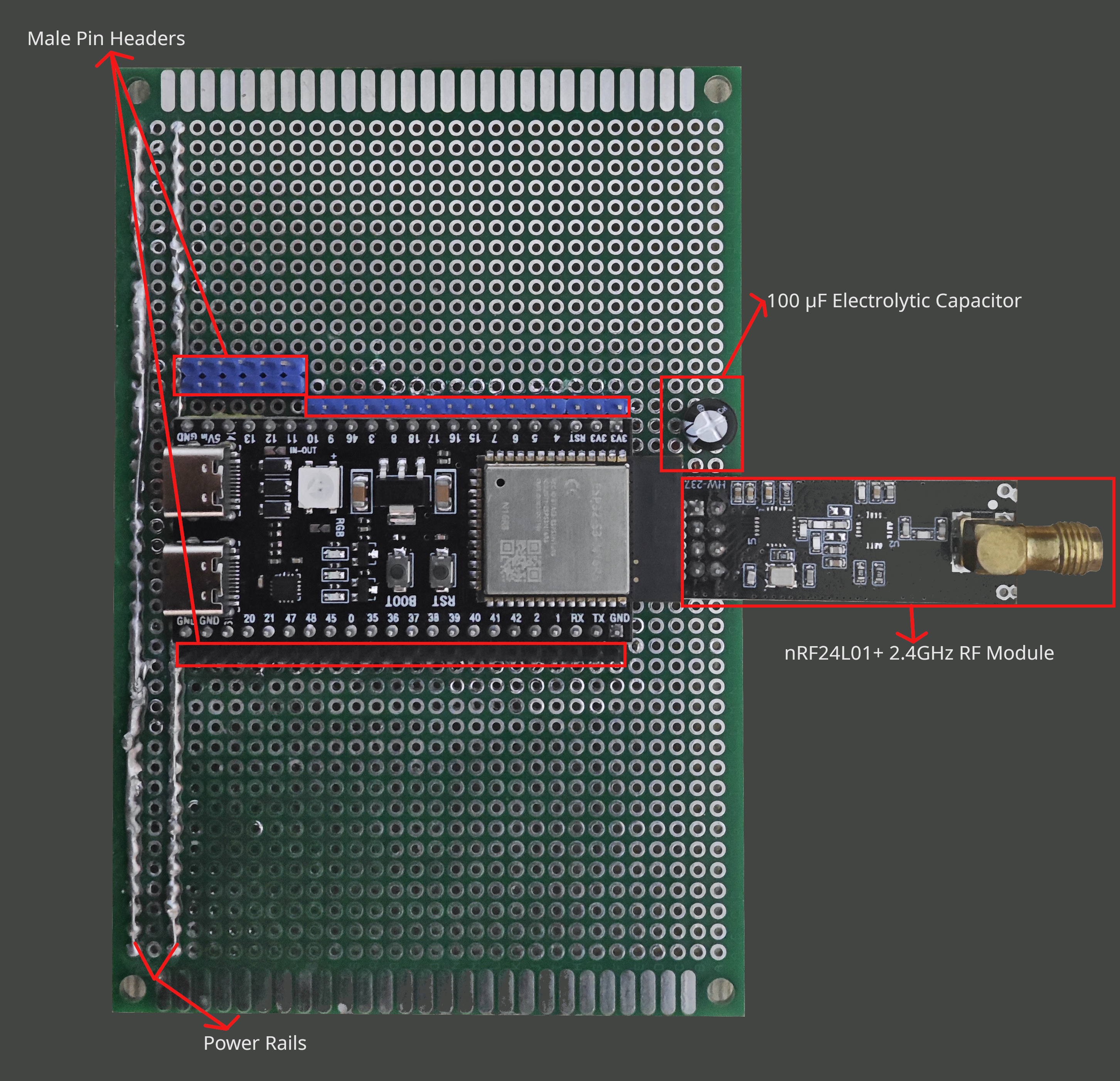
Figure 1: Phase 1 Top View — ESP32-S3-N16R8 module, nRF24L01+ RF transceiver, 100 µF bulk decoupling capacitor, peripheral male pin headers, and dedicated power rail male headers on a 6×9 cm perfboard.
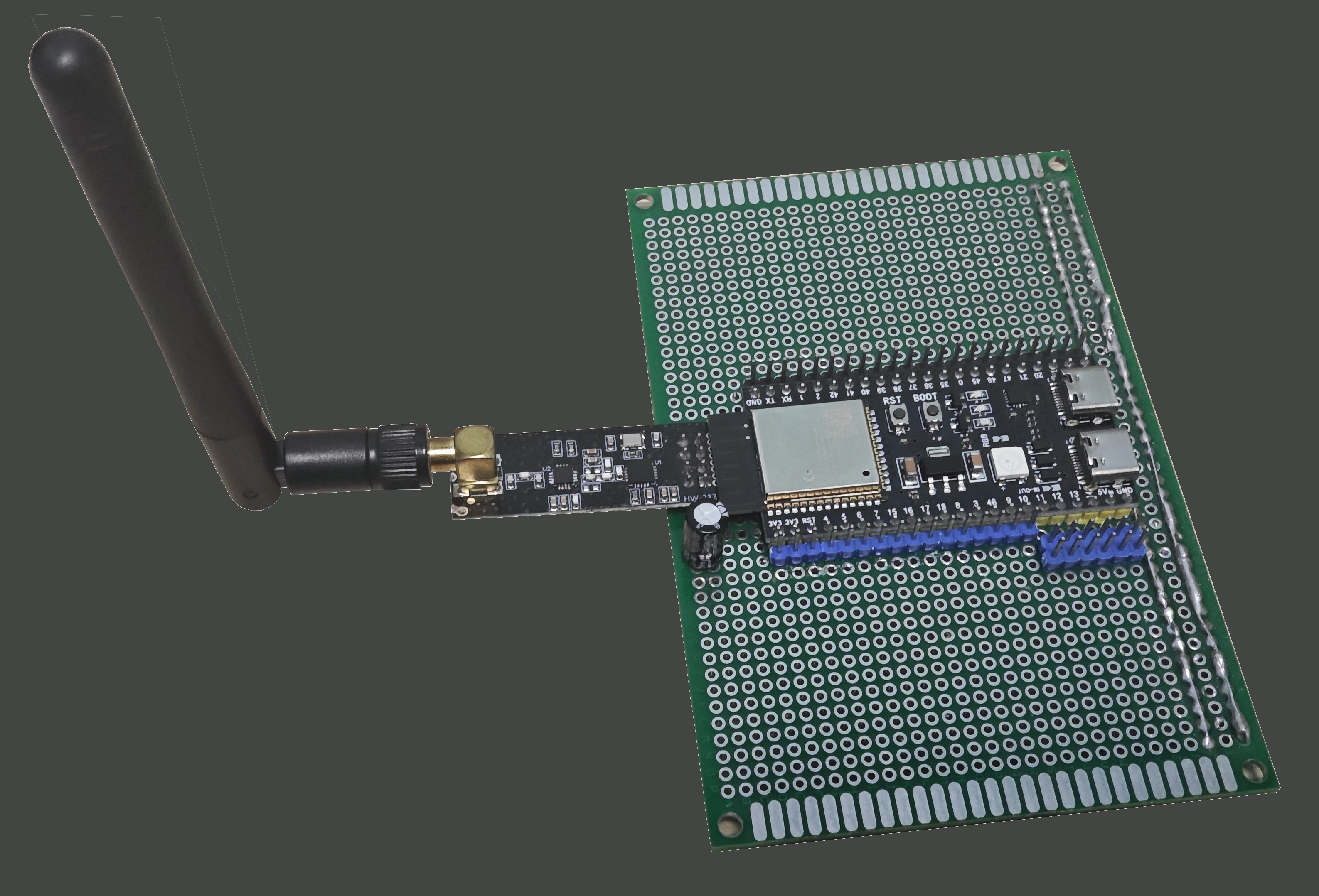
Figure 2: Phase 1 Side Profile — 2.4 GHz external dipole antenna mounted to the nRF24L01+ module and dual USB-C ports (Native USB-OTG & UART).
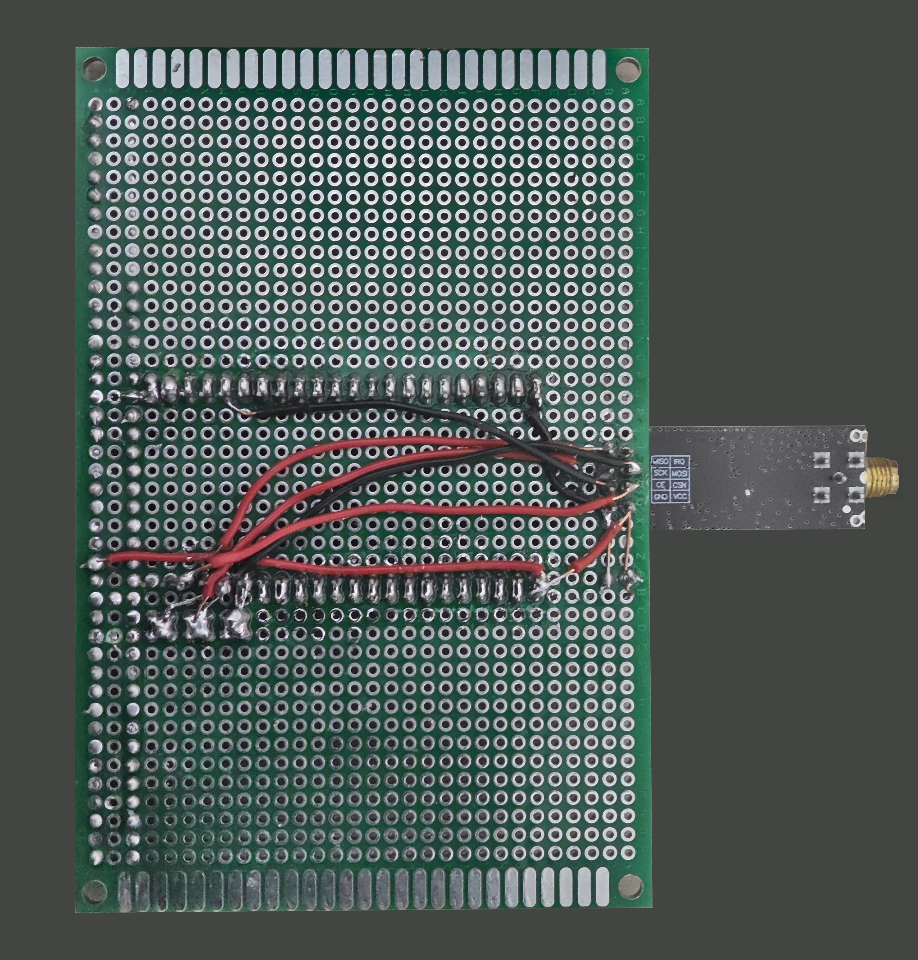
Figure 3: Phase 1 Underbody Bus Routing — Point-to-point solder bridges, common ground/power rails, and FSPI signal routing between the ESP32-S3-N16R8 and male breakout headers.
Phase 2: Console Expansion Bill of Materials (BOM)
The project is transitioning from the bare perfboard carrier into a self-contained console transmitter. Below is the complete English technical specification for the Phase 2 hardware expansion:
| Category | Component (English Technical Name) | Original / Part Spec | Engineering Role in Controller |
|---|---|---|---|
| Enclosure | DT-100 Desktop Instrument Enclosure (Black ABS) | DT-100 (190 × 137 × 59 mm) |
Main desktop/handheld transmitter chassis housing the perfboard, dual gimbals, screen, and battery pack. |
| Display | 1.3" ST7789 IPS TFT Color LCD Module | 240 × 240 px, RGB SPI, 3.3V |
High-contrast full-color IPS graphical dashboard replacing the benchtop monochrome OLED. |
| Primary Input | 2× Dual-Axis Hall-Effect Analog Joysticks | Contactless Magnetic 2-Axis | Drift-free 4-channel analog control (Throttle, Yaw, Pitch, Roll) routed to ADC1. |
| Audio Input | MAX4466 Electret Microphone Amplifier Module | Adjustable Gain, 2.4V–5.5V |
Analog voice telemetry capture and real-time audio FFT spectrum visualization on ADC1. |
| Storage | SPI MicroSD Card Reader Module | Standard SPI (MOSI/MISO/SCK/CS) |
Non-volatile storage for flight/drive telemetry logs, model profiles, and UI bitmap assets. |
| Power Boost | MT3608 2A Adjustable DC-DC Step-Up Boost Converter | 2V–24V Input, up to 28V / 2A Out |
Boosts the 3.7V Li-ion battery rail to 5V / 12V for auxiliary peripherals and switch LED illumination. |
| Master Switch | 12–24V Illuminated Waterproof Push-Button Switch | Latching ON-OFF, White LED Ring | Master system power / RF arming switch mounted on the DT-100 front panel. |
| Mode Switch | KTS-303 Mini Toggle Switch (3-Pin SPDT) | ON-OFF, Panel Mount |
Physical toggle switch for flight/drive mode selection or high/low rate switching. |
| Aux Switch | 180° Vertical Slide Switch | ON-OFF Slide, Through-Hole |
Sub-circuit power rail isolation / programming mode selector. |
| Power Diode | 1N5817 Schottky Barrier Diode | 1A, 20V, DO-41 THT |
Low forward-voltage drop (V_F \approx 0.45\text{V}) power rail OR-ing and reverse-polarity protection. |
| Rectifier Diode | 1N4001 General-Purpose Silicon Diode | 1A, 50V, DO-41 THT |
Reverse-current blocking and inductive flyback protection across switched loads. |
| Switching BJT | 2N2222 NPN Bipolar Junction Transistor | 40V, 600mA–800mA, TO-92 |
Low-side transistor switch allowing 3.3V ESP32-S3 GPIOs to drive the 12V switch LED ring (via MT3608) or buzzers. |
Verified Pin Mapping (Phase 1 Firmware & Bench Harness)
The master firmware (firmware/main/mmcontroller.c) configures a collision-free shared SPI2_HOST (FSPI) bus, ADC1 analog inputs, and the hardware pulse_cnt quadrature decoder:
| Peripheral / Signal | GPIO | Hardware Interface | Description |
|---|---|---|---|
| SPI Bus: MOSI | GPIO 11 |
SPI Master Output (SPI2_HOST) |
Shared data line for nRF24L01+, Display (SDA), and MicroSD |
| SPI Bus: MISO | GPIO 13 |
SPI Master Input (SPI2_HOST) |
Shared data input line from nRF24L01+ and MicroSD |
| SPI Bus: SCK (Clock) | GPIO 12 |
SPI Master Clock (SPI2_HOST) |
Shared clock line for nRF24L01+, Display (CLK), and MicroSD |
| nRF24L01+ Chip Select (CS) | GPIO 14 |
SPI Device Select | Dedicated radio bus enable |
| nRF24L01+ Chip Enable (CE) | GPIO 21 |
Digital Output | Radio TX/RX power state activation line |
| Display Chip Select (CS) | GPIO 10 |
SPI Device Select | Display SPI bus enable |
| Display Data/Command (DC) | GPIO 9 |
Digital Output | Display command vs. frame data selection |
| Display Reset (RES) | GPIO 8 |
Digital Output | Hardware display reset line |
| Joystick 1 VRx (X-Axis) | GPIO 4 |
ADC1 Channel 3 (12 dB Atten) |
Analog X-axis input (0–3.3V safe) |
| Joystick 1 VRy (Y-Axis) | GPIO 5 |
ADC1 Channel 4 (12 dB Atten) |
Analog Y-axis input (0–3.3V safe) |
| Rotary Encoder CLK | GPIO 15 |
ESP-IDF pulse_cnt Unit |
Quadrature channel A (hardware edge counter) |
| Rotary Encoder DT | GPIO 16 |
ESP-IDF pulse_cnt Unit |
Quadrature channel B (direction sensing) |
| Rotary Encoder Switch (SW) | GPIO 17 |
Digital Input (PULLUP) |
Push-button (menu enter/select mode) |
Silicon Multiplexing Notes (ESP32-S3-N16R8 vs. Classic ESP32)
- Octal PSRAM & Flash Reservation (
GPIO 26 – GPIO 37): On the ESP32-S3-N16R8 (8 MB Octal PSRAM),GPIO 26throughGPIO 37are wired internally to the Octal SPI Flash/PSRAM bus. AccessingGPIO 26, 27, 32, 33triggers an immediate Guru Meditation Error / Cache Disabled Panic on boot. - Unbonded Silicon Pins (
GPIO 22 – GPIO 25):GPIO 22, 23, 24, 25do not exist on the ESP32-S3 pin multiplexing matrix. - FSPI (
SPI2_HOST) Default Matrix: Uses native ESP32-S3 FSPI pins (GPIO 10, 11, 12, 13) rather than legacy 2016 ESP32 VSPI defaults (GPIO 5, 18, 23).
Repository Structure
multi-functional-controller/
├── firmware/                        # ESP-IDF C99 Firmware Project (ESP32-S3)
│   ├── CMakeLists.txt               # Top-level CMake project configuration
│   ├── sdkconfig                    # Verified ESP32-S3 target configuration
│   └── main/
│       ├── CMakeLists.txt           # Component registration
│       └── mmcontroller.c           # Master firmware: Shared SPI2, Display UI, nRF24L01+, PCNT, ADC1
├── hardware/                        # KiCad 10 Electronic Design Automation (EDA)
│   ├── mfc-1.kicad_pro              # KiCad project file
│   ├── mfc-1.kicad_sch              # Phase 1 schematic design (ESP32-S3, nRF24L01+, 100uF cap)
│   └── mfc-1.kicad_pcb              # Board layout & routing rules
├── images/                          # High-resolution Phase 1 prototype photography
│   ├── TOP_VIEW.png                 # Perfboard top view (MCU, RF, 100uF cap, male pin headers)
│   ├── SIDE_VIEW_WITH_ANTENNA.png   # RF antenna and profile perspective
│   └── BOTTOM_VIEW.png              # Perfboard underside solder bus & power rail wiring
├── .gitignore                       # Clean repository filter (builds, caches, local configs)
├── LICENSE                          # MIT License
└── README.md                        # Master engineering documentation
Getting Started: Building the Firmware
. $HOME/esp/esp-idf/export.sh
cd firmware
idf.py set-target esp32s3
idf.py build
idf.py -p /dev/ttyACM0 flash monitor
Project Status & Roadmap
- Phase 1 Hardware (Complete): 6×9 cm perfboard carrier assembly with ESP32-S3-N16R8, nRF24L01+ RF module, 100 µF decoupling capacitor, signal male headers, and power rail male headers.
- Phase 1 Firmware (Complete): Shared
SPI2_HOSTbus, 5×8 UI state machine (DRIVE VEHICLE,RADIO CONFIG,CALIBRATE,SYSTEM INFO), hardwarepulse_cntrotary decoding, and live nRF24 channel tuning (0–125). - Phase 2 Hardware Integration (In Progress):
- Mount system into DT-100 (
190 × 137 × 59 mm) black desktop enclosure. - Integrate 2× Dual-Axis Hall-Effect Joysticks (
ADC1channelsGPIO 4, 5, 6, 7). - Upgrade display to 1.3" ST7789 240×240 IPS TFT LCD.
- Wire MT3608 DC-DC Boost Converter, 1N5817 / 1N4001 Diodes, and 2N2222 NPN BJT to drive the 12–24V Illuminated Push-Button Switch, KTS-303 Toggle Switch, and 180° Slide Switch.
- Integrate MAX4466 Microphone Amplifier and SPI MicroSD Card Module.
- Mount system into DT-100 (
- Phase 3 Custom PCB: Full multi-layer PCB fabrication in KiCad 10.
Author & Project Notebook
- Author: Ertunç Özbay
- Personal Workshop & Portfolio: ertuncozbay.dev
- Project Detail Page: ertuncozbay.dev/projects/multi-functional-controller.html
- License: MIT License